8085 Circuit Diagram
8085 diagram microprocessor description pdf circuit various code chip microprocessors board address buses bit mpu general its purpose choose Inside the alu of the 8085 microprocessor 8085 programming: 8085 pin out diagram
Microprocessor - 8085 Architecture - Code Helpers
8085 diagram microprocessor configuration description pinout integrated elektropage electronics those signal technology introduction teacher electronic mechatronics circuits ic engineer clock Pin diagram of 8085 microprocessor Introduction to microprocessor 8085 and pin diagram part1 ~ engineering
8085 microprocessor edusera microprocessors
8085 architecture : pin diagram and its addressing modesIntel 8085 microprocessor architecture and programm.. Schematic microprocessor bit gate negationBlog archives.
Microprocessor intel basic addressing diagram modes8085 architecture : pin diagram and its addressing modes I need a wiring/circuit schematic of a specific 8085 starter kitPin diagram of 8085.

8085 microprocessor ic
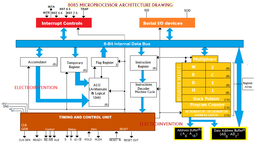
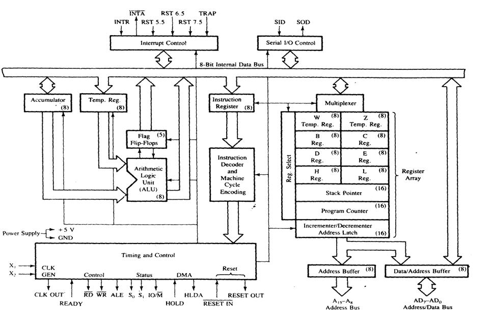
Education for all: functional block diagram of 8085 microprocessorMicroprocessor architecture 8085 diagram block functional function diagrams microprocessors 8086 structure alu computer book bus logic microcontrollers education buses electronics 8085 registers microprocessor refereeing directly respective programmer8085 pin diagram.
8085 microprocessor architecture diagram timing control address data circuitry electronics club registers instruction unit buffer machine cycle logic different decoderMicroprocessor signals 8085 microprocessor registers8085 diagram block intel processor ppt presentation powerpoint set its instruction.
What is the difference between 8085 and 8086 microprocessor
Stepper interface interfacingThe 8085 microprocessor World of embedded: pin-out diagram of 80858085 microprocessor study notes for electronics and communication.
8085 microprocessor architecture difference intel between unit control register pediaa features importantBasic microprocessor's (intel 4004 and 8085). « sadaf media A "media to get" all datas in electrical science...!!: 8085World of embedded: interfacing of 8255 with 8085 processor.

8255 8085 interfacing processor embedded
Microprocessor signals diagram supply power frequency clock engineering notes8085 microprocessor architecture intel diagram block programming Micro processor 8085 questions and answers by ramesh kumar8085 microprocessor motor dc based control speed system using controller datas electrical science.
Microprocessor diagram architecture depicts following8085 microprocessor architecture ic External memory interfacing in 8085: ram and romPin diagram of 8085 microprocessor ~ my it tutors.

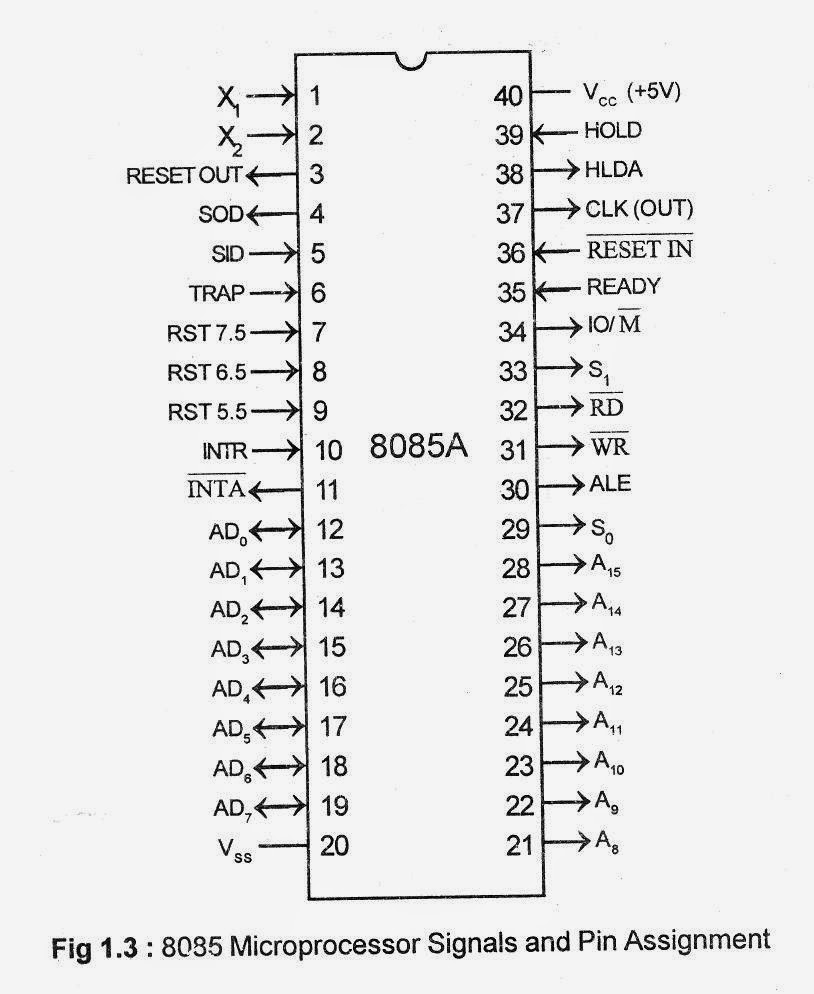
8085 pin diagram
8085 microprocessor: architecture, pin diagramMicroprocessor reset onwards 0000h executing Interfacing 8085 rom microprocessor8085 microprocessors functional signals.
8085 diagram embedded .


